
A rectangular waveguide is a hollow metal pipe that carries one electromagnetic mode at a time above a cutoff frequency. This case drives the dominant TE10 mode down a standard WR-90 guide (X-band) and reads the two-port S-parameters. An ideal empty guide should pass the mode with almost no reflection — and because the matched empty-guide answer is known in closed form, it is a clean absolute check on the waveguide port.
The structure
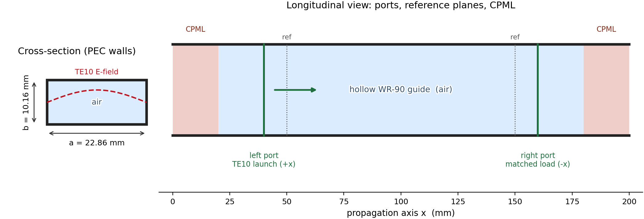
A WR-90 guide: broad wall a = 22.86 mm, narrow wall b = 10.16 mm, metal (PEC) walls, hollow air inside. The mode is launched at the left port and collected at the right port. Both end faces are absorbing (CPML); the four side walls are PEC.
What this is
The dominant mode of a rectangular guide is TE10. It only propagates above the
cutoff frequency set by the broad-wall width: f_c = c / (2·a). For WR-90,
a = 22.86 mm gives f_c ≈ 6.557 GHz, so the X-band (8.2–12.4 GHz) sits
comfortably above cutoff and the TE10 mode travels cleanly. Below f_c the mode
is evanescent and the guide rejects it. Filling the guide with a dielectric εr
lowers the cutoff to f_c,d = f_c / √εr — the lever the autodiff section below
differentiates through.
What you’ll learn
- Launching the TE10 dominant mode with a mode-matched waveguide port (a one-sided mode injection, not a soft point source).
- The cutoff relation
f_c = c/(2·a)and why X-band propagates in WR-90 while lower frequencies would not. - Reading two-port |S11| (reflection) and |S21| (transmission) against the
exact matched empty-guide answer (
|S11| = 0,|S21| = 1). - Taking a gradient through the FDTD solver with
jax.grad: how|S21|responds to the guide’s dielectric fill, validated against finite differences.
Geometry & materials
import numpy as npC0 = 299_792_458.0
a_wg = 22.86e-3        # WR-90 broad wall (sets the TE10 cutoff)b_wg = 10.16e-3        # WR-90 narrow wallf_c  = C0 / (2 * a_wg) # TE10 cutoff: c / (2a) -> 6.557 GHzdx   = 1.0e-3          # 1 mm cells -> ~30 cells/wavelength at 10 GHzfreqs = np.linspace(8.2e9, 12.4e9, 21)   # X-band sweep
The guide is hollow air inside PEC walls. The only material knob is the optional dielectric fill used in the gradient demonstration below.
Source, ports, boundaries, mesh
- Two TE10 waveguide ports. The left port (
direction="+x") launches the mode; the right port (direction="-x") acts as a matched load. Each port injects the discrete Yee-grid mode profile, so the launcher back-reflection is minimal. - CPML on the propagation axis only (20 cells). Twenty layers drive the
residual guided-mode reflection floor to essentially zero (
|S11| ≈ 0); thinning to the default 10–12 layers raises it toward ~0.09 (a known trap). Only the two x faces absorb. - PEC side walls. The four y/z walls are PEC — that is what defines a rectangular guide and its cutoff.
- Uniform 1 mm mesh. Ten cells span the narrow wall, about 23 the broad
wall, and roughly 30 cells per wavelength at the top of the band — enough to
resolve the TE10 half-sine across
aand keep numerical dispersion small.
Geometry check (before running)
The render above confirms the guide before committing compute: broad wall a, narrow wall b, the two port planes set back from the absorbers, and clearance to the CPML on both ends. An empty WR-90 run at 1 mm (about 46k cells, a few hundred steps) finishes in seconds on a CPU; peak memory is a few tens of megabytes.
Run
import numpy as np, jax.numpy as jnpfrom rfx.api import Simulationfrom rfx.boundaries.spec import Boundary, BoundarySpec
a_wg, b_wg, dx = 22.86e-3, 10.16e-3, 1.0e-3freqs = np.linspace(8.2e9, 12.4e9, 21)f0 = float(freqs.mean()); bandwidth = 0.5domain_x = 0.200
sim = Simulation(    freq_max=float(freqs[-1]) * 1.1,    domain=(domain_x, a_wg, b_wg), dx=dx,    boundary=BoundarySpec(x=Boundary(lo="cpml", hi="cpml"),                          y=Boundary(lo="pec", hi="pec"),                          z=Boundary(lo="pec", hi="pec")),    cpml_layers=20,)port_freqs = jnp.asarray(freqs)sim.add_waveguide_port(0.040, direction="+x", mode=(1, 0), mode_type="TE",    freqs=port_freqs, f0=f0, bandwidth=bandwidth,    waveform="modulated_gaussian", reference_plane=0.050, name="left")sim.add_waveguide_port(domain_x - 0.040, direction="-x", mode=(1, 0), mode_type="TE",    freqs=port_freqs, f0=f0, bandwidth=bandwidth,    waveform="modulated_gaussian", reference_plane=domain_x - 0.050, name="right")
result = sim.compute_waveguide_s_matrix(num_periods=200, normalize=True)
Run it from the command line:
python scripts/precompute_gallery_artifacts.py --case waveguide_wr90Fields
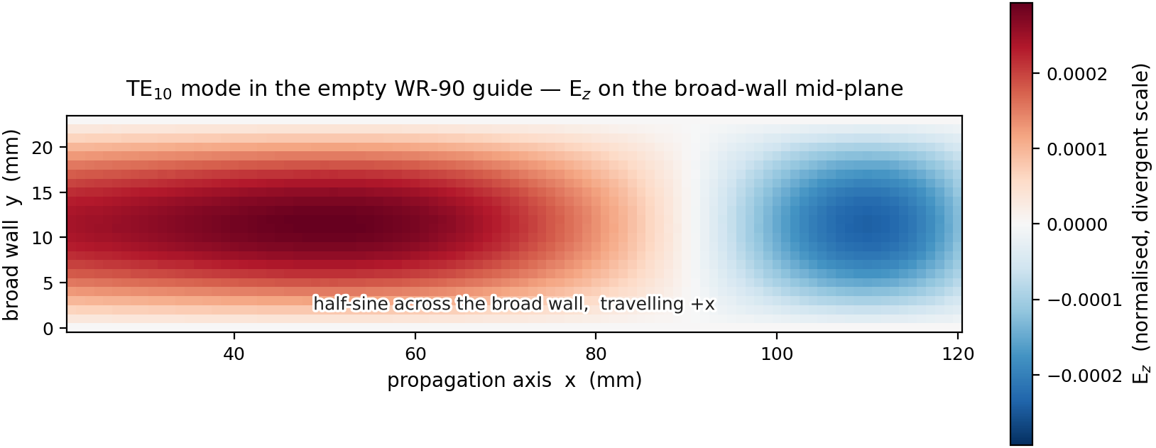
E_z on the broad-wall mid-plane of a source-fed empty guide, captured once the pulse has propagated to mid-guide. The field is a half-sine across the broad wall — peaking at the centre and vanishing at the PEC side walls — travelling in the +x direction, with the next half-cycle of opposite sign following behind. That is the TE10 mode moving down the guide.
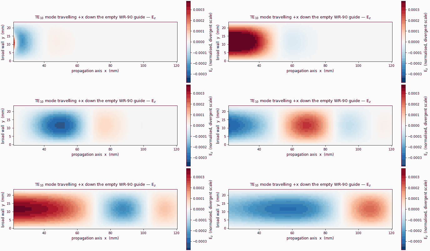
The same mode in motion: the TE10 wave packet propagates in the +x direction down the guide and into the matched absorber, holding its half-sine profile across the broad wall as it travels.
Result
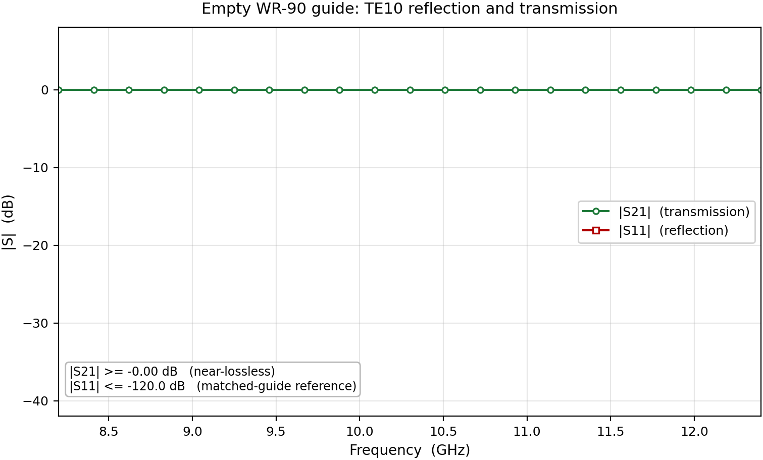
Across the X-band, |S21| sits at about 0 dB and |S11| is essentially zero
(max|S11| = 0.0000 with the thick CPML) — so the empty matched guide passes the
TE10 mode essentially perfectly, which is exactly what an ideal guide above cutoff
should do. (Thinning the absorber raises the reflection floor toward ~0.09; see
the limit note under Validation.)
Validation & limits
The empty matched guide has an exact answer: |S11| = 0 and |S21| = 1 at every
frequency above cutoff. The figure overlays the rfx values on that reference.
| Observable | rfx | Reference | Tolerance | Pass |
|---|---|---|---|---|
| max|S11| | 0.0000 | 0 (analytic matched-load) | < 0.02 | yes |
| min|S21| | 1.0000 | 1 (analytic matched-load) | > 0.97 | yes |
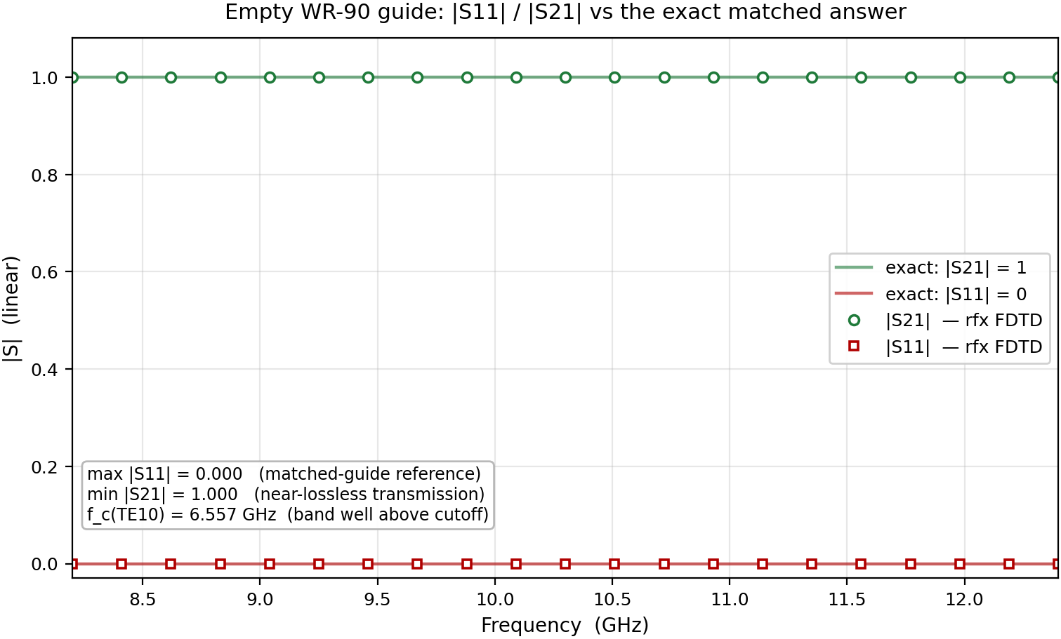
Reference: analytic matched-load (|S11| = 0, |S21| = 1 above cutoff),
cross-checked against MEEP/OpenEMS/Palace. With the thick
20-layer CPML this run produces, the published result is max|S11| = 0.0000 and
min|S21| = 1.0000 to the figure’s precision — the empty matched guide passes
the TE10 mode essentially perfectly, as an ideal guide above cutoff should.
Limit — absorber floor. The residual |S11| is a CPML back-reflection floor,
not a solver error. The 20-layer absorber holds it at the ≈0 published here;
thinning the CPML to the default 10–12 layers raises the reflection floor toward
about 0.09. So the floor is a sensitivity to the absorber thickness, not the
guide’s reflection.
Autodiff
Fill part of the guide with a dielectric and |S21| responds, and that response
is differentiable. The design variable is the fill permittivity εr, entered
through eps_override, and the scalar is |S21|². A single jax.value_and_grad
call returns ∂|S21|²/∂εr straight through compute_waveguide_s_matrix( normalize="flux", ...) — the power-flux extraction is on the AD tape, so the
gradient flows through the full modal S-matrix assembly.
There is no closed form for the filled-guide |S21|, so the AD gradient is
compared against central finite differences (h = 0.05), asking for agreement
within 5% and a matching sign.
| Check | AD value | Compared against | rel. error | Sign agrees |
|---|---|---|---|---|
∂|S21|²/∂εr | −0.2201 | central FD −0.2197 (h = 0.05) | 0.0017 (0.17%) | yes |
It agrees to 0.17% with matching sign — well inside the 5% asked of it. That
number validates the differentiation of this computation; it is not a
chain-closure verdict for the family. The rectangular-waveguide S-matrix row of
docs/guides/support_matrix.md (source checkout) records: “Chain battery:
chain-closed (v1.8) for uniform single-mode S on the normalize=False and
normalize="flux" lanes” — contract criteria 1 (forward identity) and 3(a)
(AD-vs-FD) read under JAX_ENABLE_X64 on the flux lane, the forward default
still float32. The 0.17% figure above is a float32 flux-lane gradient: the
declaration leaves a float32 gradient pipeline on that lane outside it (its
forward identity misses the contract bound at 1.08–1.76 of the allowance),
so read this page’s number as an AD-vs-FD agreement on this computation, not
as a chain-closed gradient. Chain-closed is not “supported”; the row stays
limited.
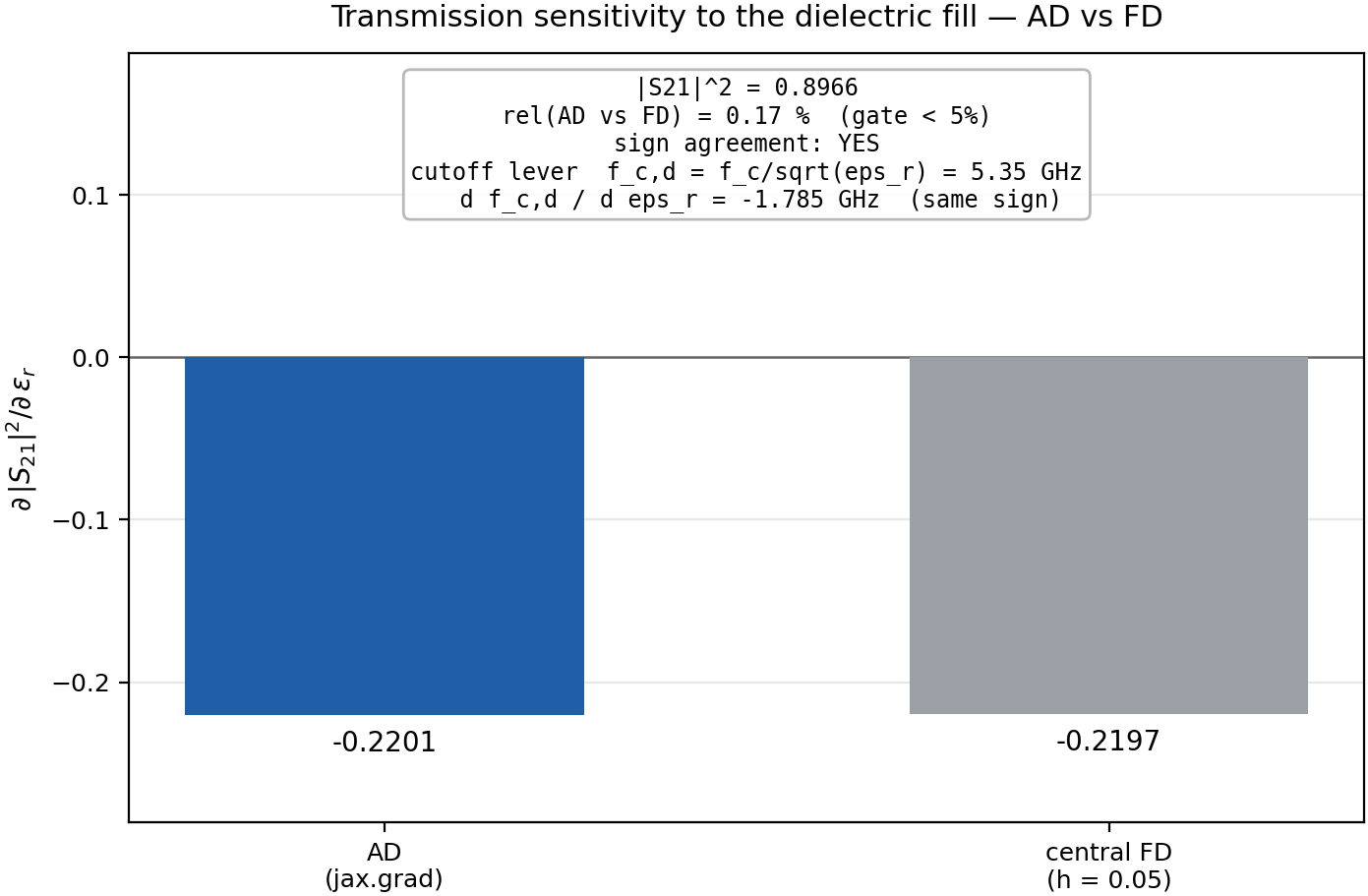
The AD gradient ∂|S21|²/∂εr ≈ −0.220 matches the central finite difference to
about 0.2 %, with matching sign. The sign is physical: a dielectric fill lowers
the cutoff toward the band through f_c,d = f_c / √εr (so
∂f_c,d/∂εr = −f_c / (2·εr^{3/2}), about −1.8 GHz), which moves the band edge
and reduces transmission. The closed-form cutoff relation points the same way the
solver gradient does.
Limits. The reflection floor is the CPML, not the physics — the 20-layer
absorber drives the published |S11| to ~0, and thinning to the default 10–12
layers raises it toward ~0.09 (a known trap). The broad-wall width a is not
a jax.grad input: a/dx is a discrete cell count and the analytic mode profile
is rebuilt for each width, so its sensitivity is shown by re-meshing and finite
differences, alongside the analytic cutoff relation f_c = c/(2·a) — not by
automatic differentiation. The differentiable lanes are normalize=False and
normalize="flux". normalize=True is the host-assembled two-run lane and is
outside the differentiable chain: it raises NotImplementedError for a traced
eps_override/sigma_override under jax.grad/jax.jit
. The Run block above passes a concrete
normalize=True and runs forward; the same call under jax.grad raises.
Next
Computed with rfx 1.6.5 · 1eb551b · generated 2026-06-30T03:22:31Z