
A rectangular waveguide is a hollow metal pipe that carries one electromagnetic mode at a time above a cutoff frequency. This case drives the dominant TE10 mode down a standard WR-90 guide (X-band) and reads the two-port S-parameters. An ideal empty guide should pass the mode with almost no reflection — and because the matched empty-guide answer is known in closed form, it is a clean absolute check on the waveguide port.
The structure
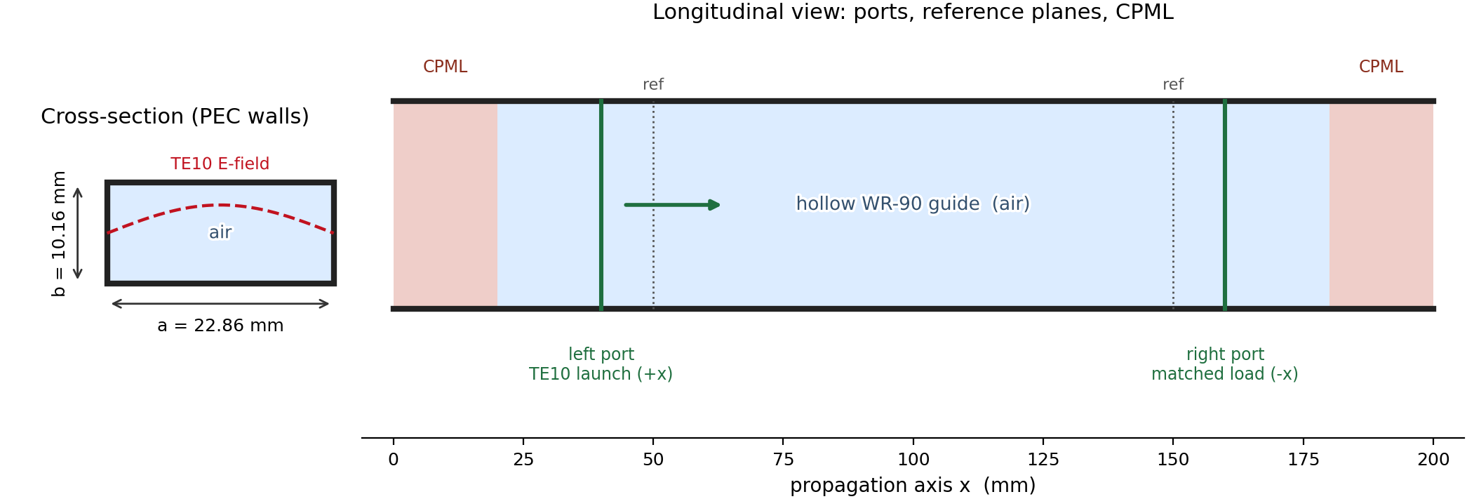
A WR-90 guide: broad wall a = 22.86 mm, narrow wall b = 10.16 mm, metal (PEC) walls, hollow air inside. The mode is launched at the left port and collected at the right port. Both end faces are absorbing (CPML); the four side walls are PEC.
What this is
The dominant mode of a rectangular guide is TE10. It only propagates above the
cutoff frequency set by the broad-wall width: f_c = c / (2·a). For WR-90,
a = 22.86 mm gives f_c ≈ 6.557 GHz, so the X-band (8.2–12.4 GHz) sits
comfortably above cutoff and the TE10 mode travels cleanly. Below f_c the mode
is evanescent and the guide rejects it. Filling the guide with a dielectric εr
lowers the cutoff to f_c,d = f_c / √εr — the lever the autodiff section below
differentiates through.
What you’ll learn
- Launching the TE10 dominant mode with a mode-matched waveguide port (a one-sided mode injection, not a soft point source).
- The cutoff relation
f_c = c/(2·a)and why X-band propagates in WR-90 while lower frequencies would not. - Reading two-port |S11| (reflection) and |S21| (transmission) against the
exact matched empty-guide answer (
|S11| = 0,|S21| = 1). - Taking a gradient through the FDTD solver with
jax.grad: how|S21|responds to the guide’s dielectric fill, validated against finite differences.
Geometry & materials
import numpy as npC0 = 299_792_458.0
a_wg = 22.86e-3        # WR-90 broad wall (sets the TE10 cutoff)b_wg = 10.16e-3        # WR-90 narrow wallf_c  = C0 / (2 * a_wg) # TE10 cutoff: c / (2a) -> 6.557 GHzdx   = 1.0e-3          # 1 mm cells -> ~30 cells/wavelength at 10 GHzfreqs = np.linspace(8.2e9, 12.4e9, 21)   # X-band sweep
The guide is hollow air inside PEC walls. The only material knob is the optional dielectric fill used in the gradient demonstration below.
Source, ports, boundaries, mesh
- Two TE10 waveguide ports. The left port (
direction="+x") launches the mode; the right port (direction="-x") acts as a matched load. Each port injects the discrete Yee-grid mode profile, so the launcher back-reflection is minimal. - CPML on the propagation axis only (20 cells). Twenty layers keep the
absorber’s residual reflection of the guided mode to essentially zero
(
|S11| ≈ 0); a thinner absorber leaves a larger floor. Only the two x faces absorb. - PEC side walls. The four y/z walls are PEC — that is what defines a rectangular guide and its cutoff.
- Uniform 1 mm mesh. Ten cells span the narrow wall, about 23 the broad
wall, and roughly 30 cells per wavelength at the top of the band — enough to
resolve the TE10 half-sine across
aand keep numerical dispersion small.
Geometry check (before running)
The render above confirms the guide before committing compute: broad wall a, narrow wall b, the two port planes set back from the absorbers, and clearance to the CPML on both ends. An empty WR-90 run at 1 mm (about 46k cells, a few hundred steps) finishes in seconds on a CPU; peak memory is a few tens of megabytes.
Run
import numpy as np, jax.numpy as jnpfrom rfx.api import Simulationfrom rfx.boundaries.spec import Boundary, BoundarySpec
a_wg, b_wg, dx = 22.86e-3, 10.16e-3, 1.0e-3freqs = np.linspace(8.2e9, 12.4e9, 21)f0 = float(freqs.mean()); bandwidth = 0.5domain_x = 0.200
sim = Simulation(    freq_max=float(freqs[-1]) * 1.1,    domain=(domain_x, a_wg, b_wg), dx=dx,    boundary=BoundarySpec(x=Boundary(lo="cpml", hi="cpml"),                          y=Boundary(lo="pec", hi="pec"),                          z=Boundary(lo="pec", hi="pec")),    cpml_layers=20,)port_freqs = jnp.asarray(freqs)sim.add_waveguide_port(0.040, direction="+x", mode=(1, 0), mode_type="TE",    freqs=port_freqs, f0=f0, bandwidth=bandwidth,    waveform="modulated_gaussian", reference_plane=0.050, name="left")sim.add_waveguide_port(domain_x - 0.040, direction="-x", mode=(1, 0), mode_type="TE",    freqs=port_freqs, f0=f0, bandwidth=bandwidth,    waveform="modulated_gaussian", reference_plane=domain_x - 0.050, name="right")
result = sim.compute_waveguide_s_matrix(num_periods=200, normalize=True)
Run it from the command line:
python scripts/precompute_gallery_artifacts.py --case waveguide_wr90Fields
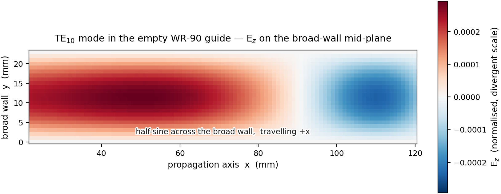
E_z on the broad-wall mid-plane of a source-fed empty guide, captured once the pulse has propagated to mid-guide. The field is a half-sine across the broad wall — peaking at the centre and vanishing at the PEC side walls — travelling in the +x direction, with the next half-cycle of opposite sign following behind. That is the TE10 mode moving down the guide.
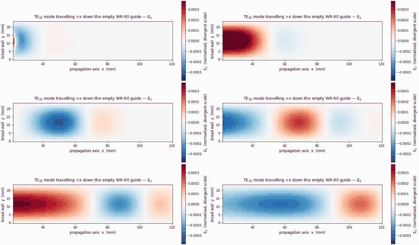
The same mode in motion: the TE10 wave packet propagates in the +x direction down the guide and into the matched absorber, holding its half-sine profile across the broad wall as it travels.
Result
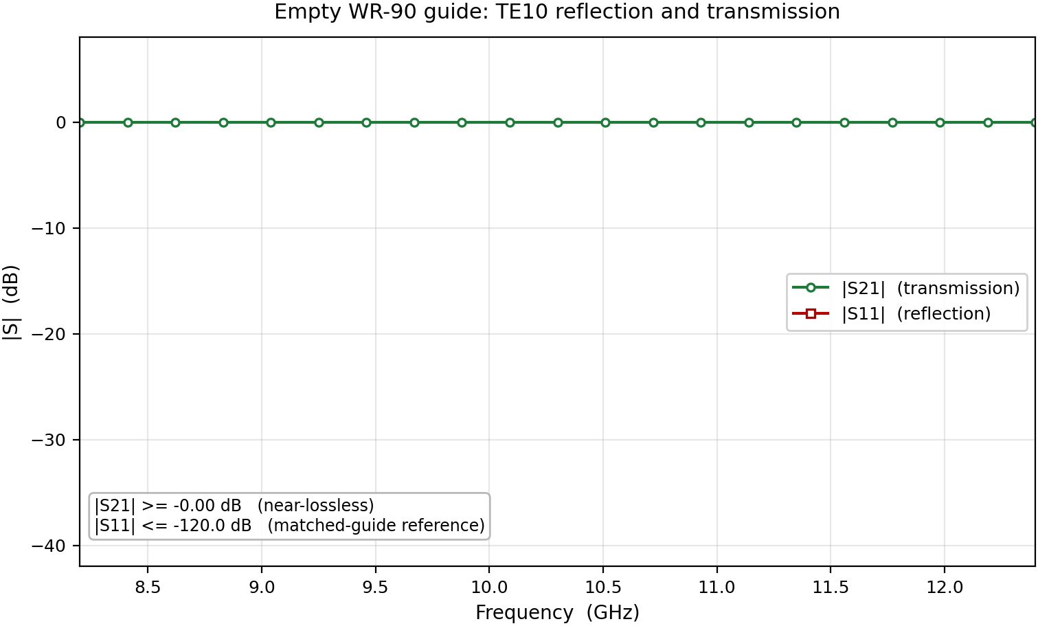
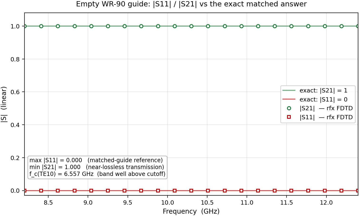
Across the X-band |S21| sits at about 0 dB and max|S11| = 0.0000 with the
20-layer CPML. An empty matched guide above cutoff should pass the TE10 mode with
no reflection, and it does.
Validation & limits
The empty matched guide has an exact answer: |S11| = 0 and |S21| = 1 at every
frequency above cutoff. The figure overlays the rfx values on that reference.
| Observable | rfx | Reference | Tolerance | Pass |
|---|---|---|---|---|
| max|S11| | 0.0000 | 0 (analytic matched-load) | < 0.02 | yes |
| min|S21| | 1.0000 | 1 (analytic matched-load) | > 0.97 | yes |
Reference: analytic matched-load (|S11| = 0, |S21| = 1 above cutoff),
cross-checked against MEEP/OpenEMS/Palace.
Limit — absorber floor. The residual |S11| is CPML back-reflection, not a
solver error. The 20-layer absorber holds it at the ≈0 published here; a
thinner absorber raises the floor. That floor tracks the absorber thickness,
not the guide’s reflection. These assets predate the 2.0 absorber correction,
which lowered the CPML’s reflection at every layer count.
Autodiff
Fill part of the guide with a dielectric and |S21| responds, and that response
is differentiable. The design variable is the fill permittivity εr, entered
through eps_override, and the scalar is |S21|². A single jax.value_and_grad
call returns ∂|S21|²/∂εr straight through compute_waveguide_s_matrix( normalize="flux", ...) — the power-flux extraction is on the AD tape, so the
gradient flows through the full modal S-matrix assembly.
There is no closed form for the filled-guide |S21|, so the AD gradient is
compared against central finite differences (h = 0.05), asking for agreement
within 5% and a matching sign.
| Check | AD value | Compared against | rel. error | Sign agrees |
|---|---|---|---|---|
∂|S21|²/∂εr | −0.2201 | central FD −0.2197 (h = 0.05) | 0.0017 (0.17%) | yes |
The gradient agrees to 0.17% with matching sign, inside the 5% this check asks for. It checks the differentiation of this one computation, not the whole waveguide family. The waveguide S-matrix is limited in the support matrix: its gradient checks were closed with 64-bit JAX on the flux lane, and this 0.17% is a float32 gradient, which sits outside that closure.
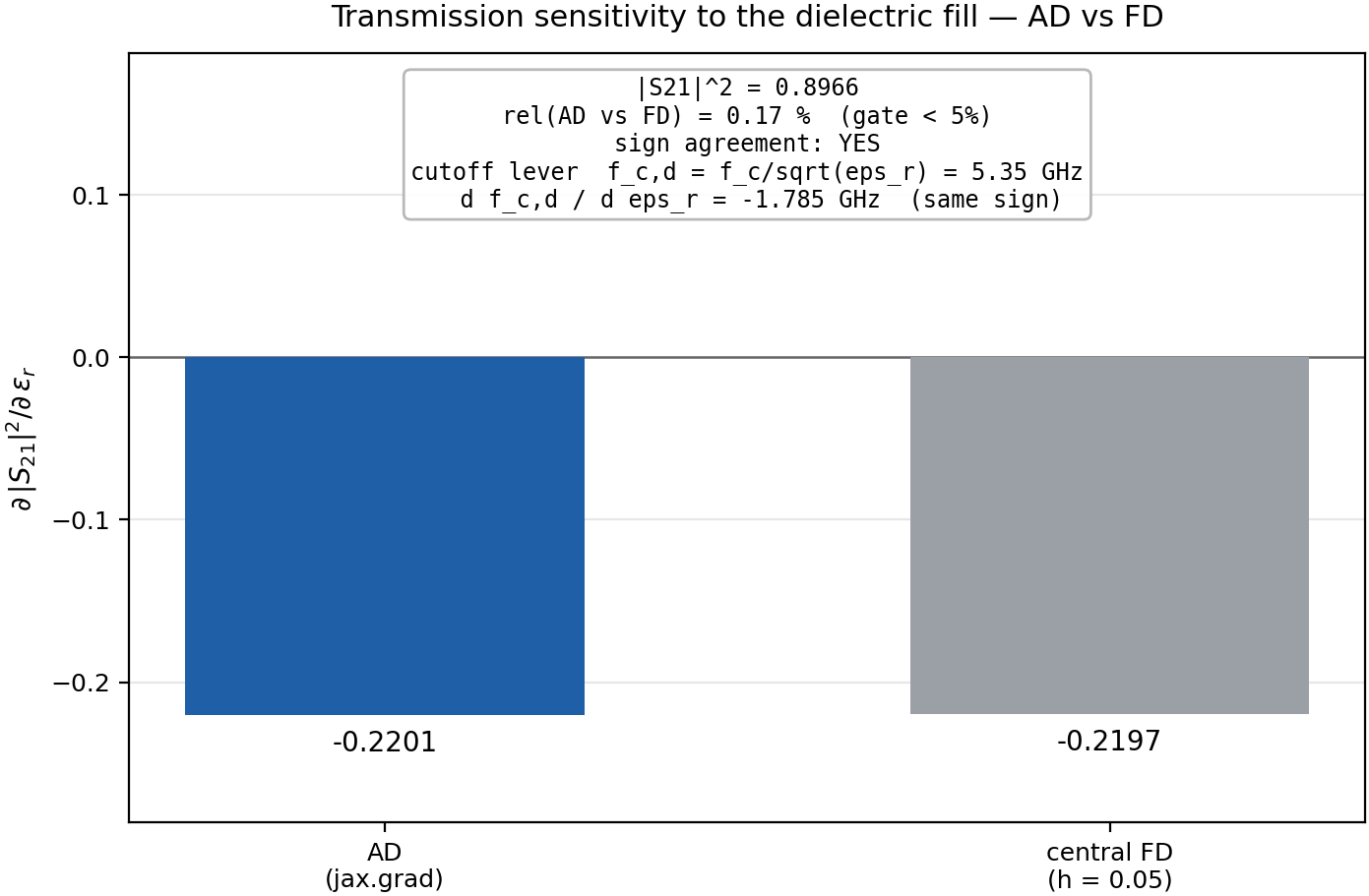
The sign is physical: a dielectric fill lowers the cutoff toward the band through
f_c,d = f_c / √εr (so ∂f_c,d/∂εr = −f_c / (2·εr^{3/2}), about −1.8 GHz),
which moves the band edge and reduces transmission. The closed-form cutoff
relation points the same way the solver gradient does.
Limits. The broad-wall width a is not a jax.grad input: a/dx is a
discrete cell count and the analytic mode profile is rebuilt for each width, so
its sensitivity comes from re-meshing and finite differences, alongside the
analytic cutoff relation f_c = c/(2·a) — not from automatic differentiation.
The differentiable lanes are normalize=False and normalize="flux".
normalize=True is the host-assembled two-run lane and is outside the
differentiable chain: under jax.grad/jax.jit, a traced
eps_override/sigma_override makes compute_waveguide_s_matrix raise
NotImplementedError before any FDTD run. The Run block above passes a concrete
normalize=True and runs forward; the same call under jax.grad raises.
Next
Computed with rfx 1.6.5 · 1eb551b · generated 2026-06-30T03:22:31Z