Skip to content

Rectangular microstrip patch antenna (2.4 GHz, FR4)

A half-wavelength rectangular microstrip patch on an FR4 substrate over a finite ground plane, fed by a single probe. It is the workhorse printed radiator for the 2.4 GHz band. The resonant length is set by the half-wave condition in the substrate’s effective permittivity: L ≈ c / (2·f₀·√ε_eff) − 2·ΔL.

  • Building a finite ground plane (a PEC box below the substrate, not an infinite pec_face) so the structure radiates instead of behaving as a closed cavity.
  • Tuning the feed inset to match the patch to 50 Ω — the input resistance falls from a high value at the radiating edge toward the patch centre, and the inset picks off the 50 Ω point.
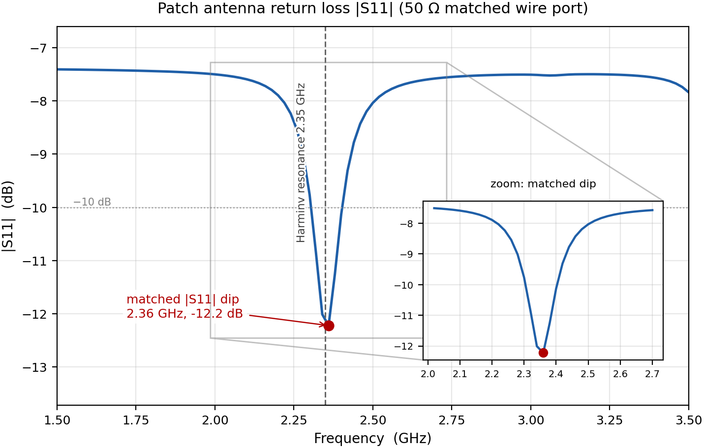
  • Reading the |S11| return loss from a 50 Ω port and seeing a deep, matched dip land at the resonance.
  • Confirming that resonance independently with a Harminv ring-down (filter diagonalisation), and cross-checking against the first-order transmission-line estimate.

The patch dimensions follow the standard transmission-line synthesis. Express them as code so they stay tied to the design frequency:

import numpy as np
C0 = 299_792_458.0
f0 = 2.4e9 # design frequency
eps_r = 4.3 # FR4 relative permittivity
h = 1.5e-3 # substrate thickness
tan_d = 0.02 # FR4 loss tangent
W = 38.0e-3 # patch width
L = 29.5e-3 # patch length
eps_eff = (eps_r + 1) / 2 + (eps_r - 1) / 2 * (1 + 12 * h / W) ** -0.5
dL = 0.412 * h * ((eps_eff + 0.3) * (W / h + 0.264)) \
/ ((eps_eff - 0.258) * (W / h + 0.8)) # fringing extension
# FR4 conductivity from the loss tangent (finite, physical Q)
sigma_fr4 = 2 * np.pi * f0 * 8.854e-12 * eps_r * tan_d
# -> W = 38.0 mm, L = 29.5 mm, eps_eff = 4.01, dL = 0.70 mm

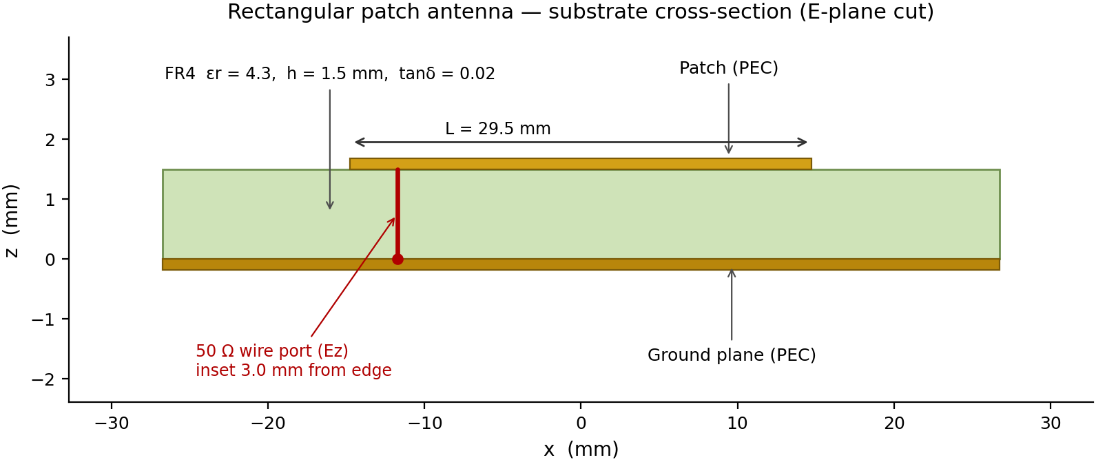
The patch is W = 38.0 mm × L = 29.5 mm on a 1.5 mm FR4 board with ε_eff ≈ 4.01. The probe feed is inset from the radiating edge so its input resistance lands near 50 Ω.

Patch antenna substrate cross-section

  • 50 Ω wire port spanning the substrate from the ground plane to the patch at the feed inset — it loads the structure with a reference impedance, so the reflection is read directly as |S11|. A multi-cell wire port (rather than a single-cell lumped port) ties the port reference plane cleanly between the two conductors, which is what lets the match show up as a deep dip.
  • 6-face CPML. The patch radiates into all six faces, so every face is absorbing; the open domain below the finite ground plane is where the antenna radiates.
  • Finite ground plane. The ground is an explicit finite PEC box beneath the substrate; the half-space below it radiates into the bottom CPML, which is the correct picture for a real patch.
  • Uniform 1 mm mesh. A single uniform mesh resolves the patch with ~30 cells across L (the TM010 half-wave is well sampled) and — unlike a non-uniform z-profile — lets the same run capture the field snapshots used below, so the return-loss dip, the Harminv resonance and the field map all come from one self-consistent simulation.

The render below confirms the stack before committing compute: patch over substrate, finite ground plane, the probe feed at the matched inset, and clearance to the CPML on every face.

Patch geometry and CPML margin check

A run of this size (≈130k cells at 1 mm, a few thousand steps) finishes in about a minute on a CPU and seconds on a GPU; peak memory is well under a gigabyte.

The construction below mirrors examples/crossval/05_patch_antenna.py, on a single uniform mesh. The 50 Ω wire port drives the patch and reads |S11|; a separate broadband-source run on the same geometry feeds the Harminv ring-down.

import numpy as np, jax.numpy as jnp
from rfx import Simulation, Box
from rfx.sources.sources import GaussianPulse
dx = 1.0e-3
air_below, air_above = 8.0e-3, 16.0e-3
gx, gy = 60.0e-3, 55.0e-3 # finite ground plane
dom_x, dom_y = gx + 16e-3, gy + 16e-3
dom_z = air_below + h + air_above
sim = Simulation(freq_max=4e9, domain=(dom_x, dom_y, dom_z), dx=dx,
boundary="cpml", cpml_layers=8)
sim.add_material("fr4", eps_r=eps_r, sigma=sigma_fr4)
z_gnd_lo = air_below - dx/2
z_sub_lo, z_sub_hi = air_below, air_below + h
gx_lo, gy_lo = (dom_x - gx) / 2, (dom_y - gy) / 2
px_lo, py_lo = dom_x / 2 - L / 2, dom_y / 2 - W / 2
sim.add(Box((gx_lo, gy_lo, z_gnd_lo), (gx_lo+gx, gy_lo+gy, z_sub_lo)), material="pec") # ground
sim.add(Box((gx_lo, gy_lo, z_sub_lo), (gx_lo+gx, gy_lo+gy, z_sub_hi)), material="fr4") # substrate
sim.add(Box((px_lo, py_lo, z_sub_hi),
(px_lo+L, py_lo+W, z_sub_hi + dx/2)), material="pec") # patch
# matched 50 ohm wire port: ground -> patch at the tuned inset
inset = 3.0e-3
sim.add_port(position=(px_lo + inset, dom_y/2, z_sub_lo), component="ez",
impedance=50.0, extent=z_sub_hi - z_sub_lo,
waveform=GaussianPulse(f0=f0, bandwidth=1.0))
result = sim.run(n_steps=7000, compute_s_params=True,
s_param_freqs=jnp.linspace(1.5e9, 3.5e9, 101), s_param_n_steps=7000)
s11 = np.asarray(result.s_params)[0, 0]
print(f"|S11| dip {20*np.log10(np.abs(s11)).min():.1f} dB")

Run it from the command line:

Terminal window
python examples/crossval/05_patch_antenna.py

E_z on the patch mid-plane at resonance, extracted as the modal phasor (a single-bin temporal DFT over the ring-down). The standing wave is the TM010 mode: a half-wave variation of E_z along the resonant length L, the two radiating edges in antiphase, a null down the patch centre, and near-uniform field along the width W. A divergent colormap with fixed symmetric limits makes the sign reversal explicit. Because this is the same uniform mesh as the |S11| run, the field map sits at the same resonance as the return-loss dip.

E_z standing wave on the patch plane at resonance

Over one RF period the mode oscillates in place: the two radiating edges swap sign through a zero crossing (E_z → 0 at the quarter period) and back — the standing-wave signature of the TM010 resonance, not a travelling wave.

Animation: the TM010 standing wave oscillating over one RF period

|S11| of the 50 Ω port across 1.5–3.5 GHz. With the feed inset tuned to 3.0 mm from the radiating edge, the port sees close to 50 Ω at resonance and the return loss drops to a deep, matched dip of −12.2 dB at 2.36 GHz — right at the TM010 resonance (dashed line). The dashed line is rfx’s own Harminv ring-down resonance; the matched dip and the ring-down coincide to within about 0.5% because the feed is matched — both are rfx reads of the same run, not an external reference.

Patch antenna |S11| in dB with the matched dip

The quantity under test is the rfx resonance frequency, checked against the first-order analytic transmission-line (Balanis) estimate. The rfx numbers below are read from the simulation itself, not from an independent solver.

ObservablerfxReferenceAgreementPass
Resonance frequency2.360 GHz (|S11| dip)2.423 GHz (analytic transmission-line, Balanis)within 20%yes
Resonance error vs reference2.6%within 20%yes
Passivitymax |S11| ≤ 1.05no gain (5% numerical margin)yes

rfx |S11|-dip resonance vs the analytic transmission-line estimate

The checked quantity is |rfx resonance − analytic|, which is 2.6% — comfortably inside the 20% agreement one can ask of a first-order estimate. The Harminv ring-down and the matched |S11| dip are both read from the rfx run itself; that these two independent reads of the same simulation land at essentially the same frequency (about 2.36 GHz) confirms the feed match is real and the dip is a meaningful operating point. A few-percent offset from the analytic number is expected: its closed-form ΔL undercounts the fringing extension, and it ignores the finite-ground and probe-feed loading.

Convergence. Refining the uniform mesh and tightening the absorber shifts the extracted resonance by a few percent at most; the coarse 1 mm mesh already places the matched dip and the ring-down resonance on top of each other, which is the self-consistency that matters here. The substrate is thin relative to the cells, so the absolute frequency carries a coarse-mesh bias — a finer mesh (a GPU pass at 0.25–0.5 mm) tightens the absolute number without changing the picture.

The same matched patch can be differentiated. The design variable is the FR4 substrate permittivity εr, and the scalar is the return loss |S11|² at the resonance. The permittivity enters through eps_override, and |S11| is read with the wave-decomposition objective minimize_s11_at_freq_wave_decomp, which runs inside Simulation.forward(port_s11_freqs=...) — the AD-traceable path that accumulates the port voltage/current DFTs inside the time-stepping loop. A single jax.value_and_grad call then returns ∂|S11|²/∂εr through this supported time-domain S-parameter workflow.

Unlike the slab, the patch has no closed-form return loss, so there is no exact derivative to compare against. Instead the AD gradient is checked against central finite differences: re-running the forward at εr ± h and forming the central difference must land within 5% of the AD gradient and point the same way.

CheckAD valueCompared againstrel. errorSign agrees
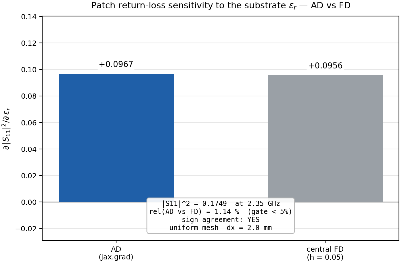
∂|S11|²/∂εr+0.0967central FD +0.0956 (h = 0.05)0.0114 (1.1%)yes

It does — 1.1% with matching sign, well inside the 5% agreement asked of it.

Patch return-loss sensitivity to the substrate permittivity — AD gradient vs central finite differences

The AD gradient ∂|S11|²/∂εr ≈ +0.097 matches the central finite difference to about 1 %, with matching sign: raising the substrate permittivity pushes the resonance down and away from the drive frequency, so the match degrades and |S11| at the fixed test frequency rises. This check runs on a uniform 2 mm mesh — coarser than the 1 mm S-parameter sweep above, since the gradient solve plus the two finite-difference forwards is heavier — but the AD-versus-finite-difference agreement it demonstrates does not depend on the mesh.

The differentiable knob is the substrate permittivity, a material quantity. The patch geometry — the feed inset along the resonant length, the patch dimensions, the mesh cell counts — is discrete and is not a jax.grad input; its sensitivity is the job of a finite-difference sweep (re-meshing and re-running), not of automatic differentiation.

Computed with rfx · 2026-06-25