
Earlier visual material, kept for reference. Current results are in the Showcase.
Choose a physical question. Each example connects a model to the motion or response it produces, with its source and evidence scope alongside the picture. The site plays stored results; it does not run a solver in your browser.
6 visual examples
Start with a field
These teaching examples were generated for this documentation update using the public Simulation API. They show actual time-domain snapshots on a single mesh; they are not convergence or RF-accuracy benchmarks.
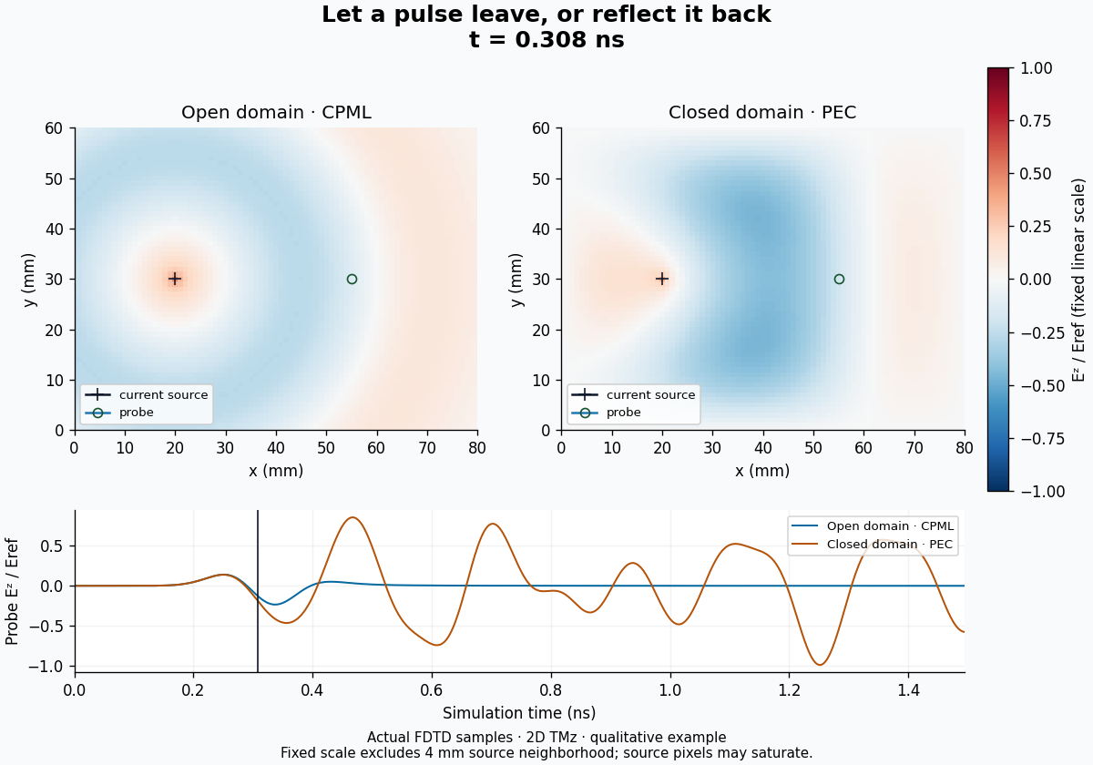
Open space or reflecting walls?
The same pulsed source with absorbing CPML boundaries and metal PEC walls.
Compare the boundaries →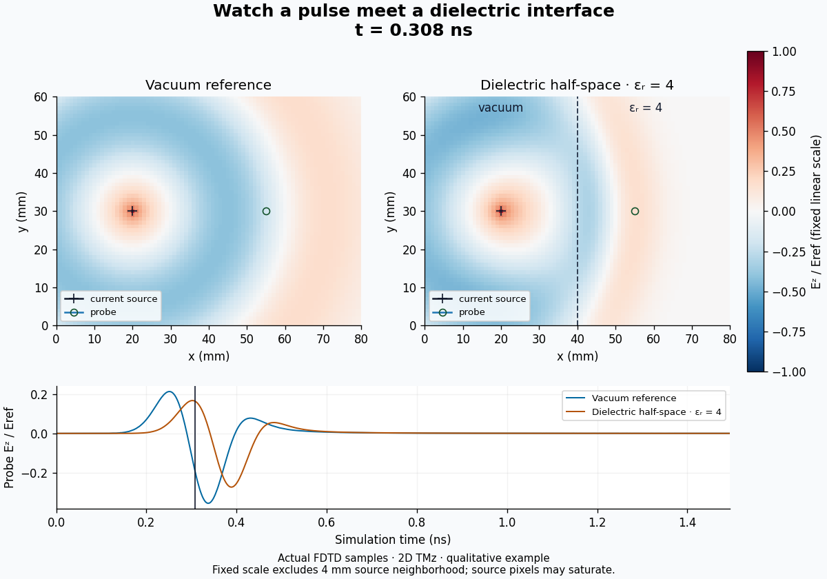
Meet a dielectric interface
Watch the field respond when the medium changes, with a vacuum comparison.
Follow the pulse →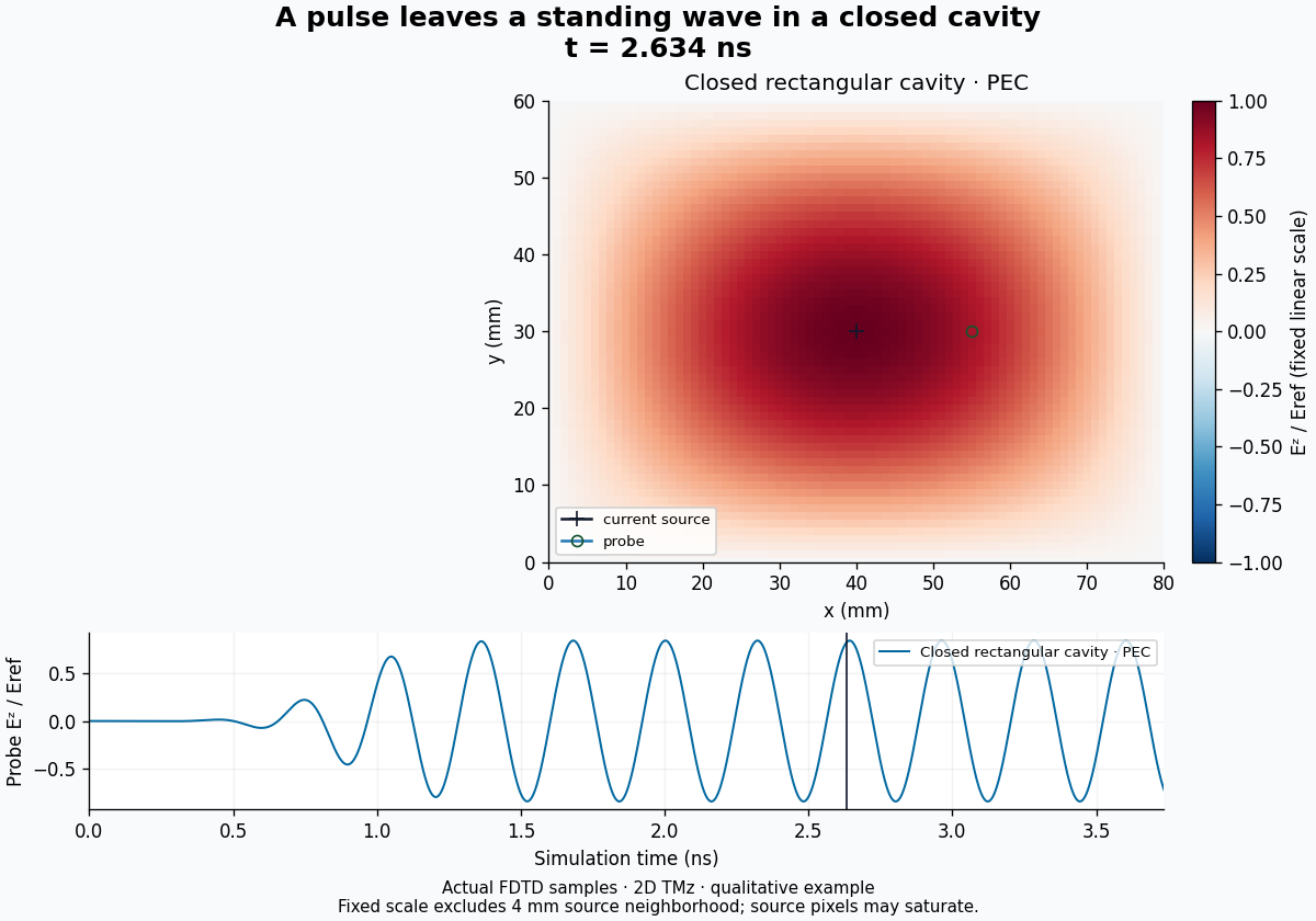
Trap a field in a cavity
See reflections and interference inside a closed conducting domain.
Watch the cavity →Explore a design in motion
These archived presentation films show more complex structures and optimization histories. Their original numbers are historical; the case pages distinguish phasor replay, real iterations and explanatory interpolation.
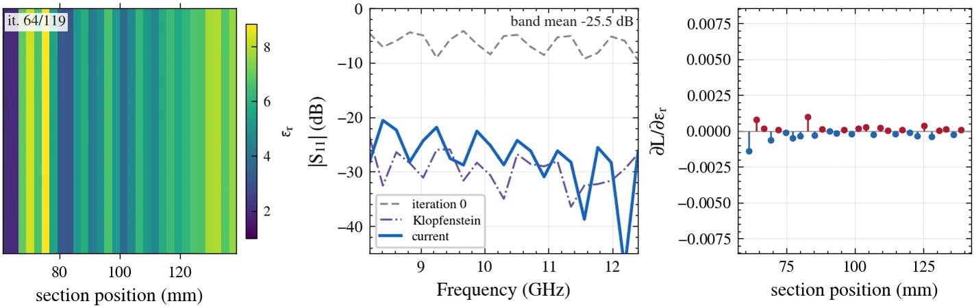
2026 paper, original films
Waveguide dielectric taper
Connect a graded material profile to broadband reflection and its sensitivity.
Watch the taper →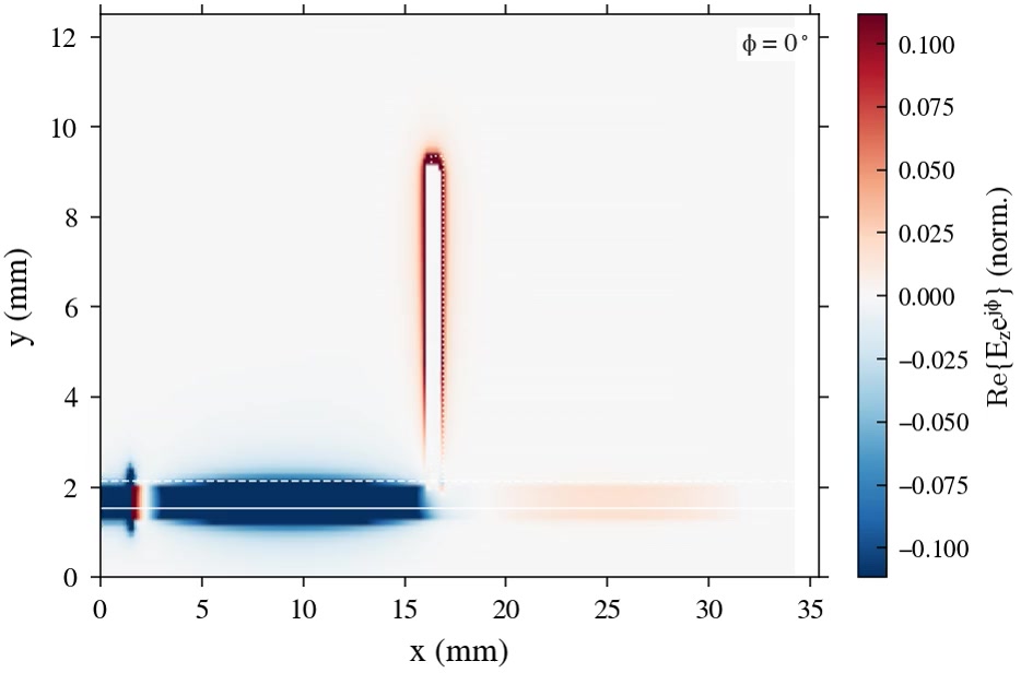
2026 paper, original films
Microstrip notch filter
Relate one geometric variable to a resonant branch and its local field.
Watch the filter →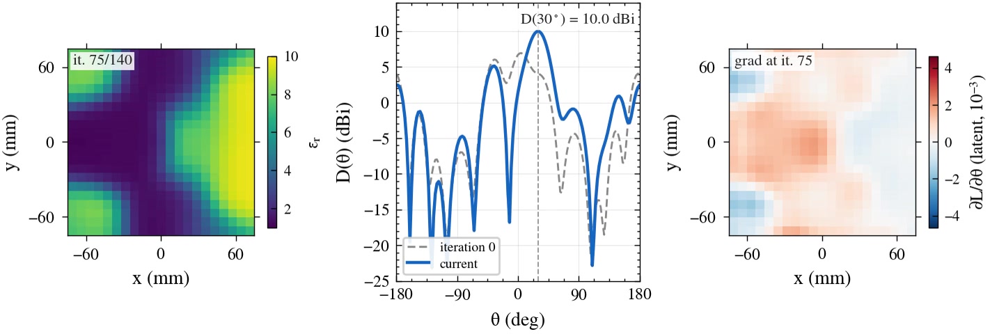
2026 paper, original films
Dielectric beam steering
Follow a spatial material pattern as the main radiation lobe changes direction.
Watch the beam →Read a reference comparison
The earlier dielectric-slab gallery and
empty rectangular-waveguide gallery retain their
field, response and derivative artifacts. Both bundles were computed with
rfx 1.6.5 at 1eb551b. Conductor placement and absorber behavior have changed
since that version, so their recorded results are not current-version benchmarks.
Read each page’s precise limits and measurement definitions.
The patch-antenna diagnostic archive is preserved for traceability. Its stored port setup does not pass current preflight; it is not a validated antenna showcase.
More visual experiments to build
These are extensions to develop and validate, not additional films already published. Their source examples provide a starting point.
| Physical question | A useful next visualization | Starting point |
|---|---|---|
| What does a dispersive material do to a pulse? | Synchronized field slices, probe traces and material response | Materials example |
| How does a radiator’s near field become a far-field pattern? | Fixed-scale field movie beside the angular radiation cut | Antenna pattern example |
| Which field is actually scattered? | Total and incident-subtracted fields beside angular RCS | Scattering example |
| How do coating layers interfere? | Layer permittivities, a field slice and the full reflection band at the same iteration | Coating example |
To build your own, follow the visual manual, choose a runnable example and keep the model, arrays and plots together.