
Choose by what you want to see
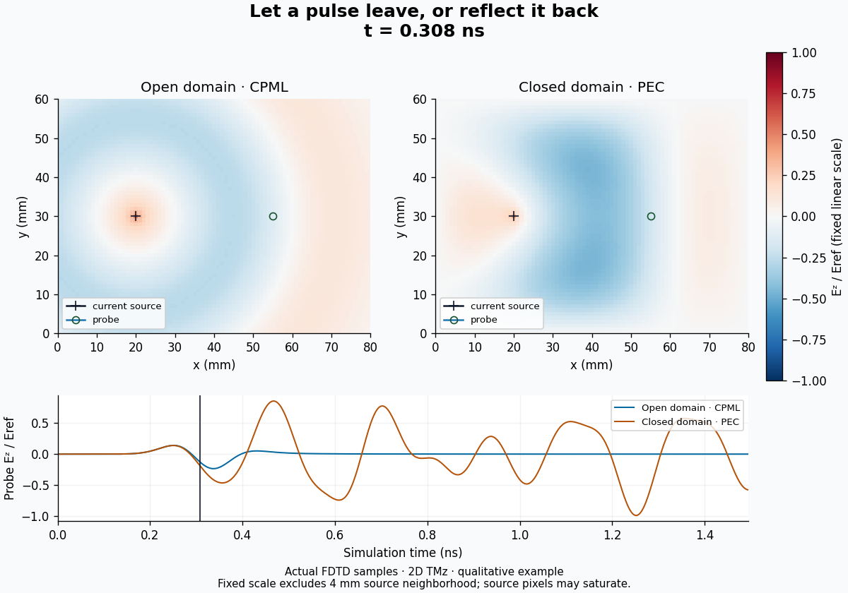
Follow a field
Begin with a pulse, a boundary and a dielectric interface. Actual time-domain snapshots make a useful first experiment.
Watch and run →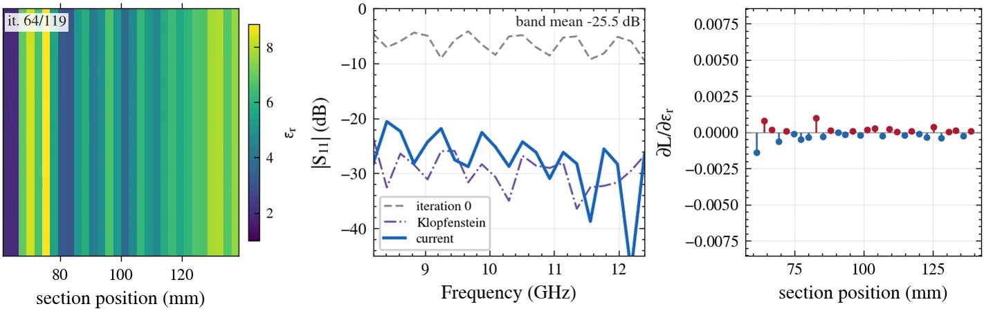
Connect structure to response
Explore historical films of a guided-wave taper or microstrip filter, then use the related source examples.
Explore RF components →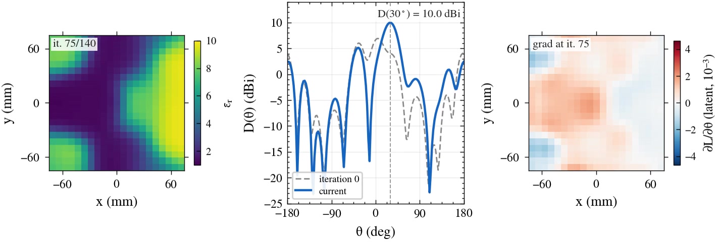
Shape the radiation
See a dielectric cover change a beam’s direction, and learn which variables its sensitivity plot describes.
Explore a design history →New to the API? Start with the first runnable model and the visual manual.
Run from a source checkout
The scripts below ship in a source checkout under examples/. Run them in
order: each one teaches one decision a real design needs. The last column says
which ports and boundaries the script builds, so you can find the one closest
to your structure. Paths in the tables are relative to examples/.
Run a script from the repository root, for example:
python examples/quickstart/hello_world.pyMost finish in seconds to a few minutes on a CPU. Steps 4 and 10 take tens of minutes.
The machine-readable index lists builders and output files.
The learning path
| # | Script | What it teaches | Ports and boundaries |
|---|---|---|---|
| 1 | quickstart/hello_world.py | install check: the smallest Simulation → run → probe loop | PEC box; point source and one probe |
| 2 | tutorials/boundary_spec_demo.py | choosing boundaries: CPML for open problems, PEC for closed ones, PMC symmetry, periodic cells; and declaring metal inside the domain as a sheet, a volume or a wire | BoundarySpec per axis and face; point source and probe |
| 3 | tutorials/slab_rt_flux_monitor.py | reflection and transmission spectra done right: flux monitors plus a reference run, and why a probe FFT misleads | CPML; plane wave; two flux monitors |
| 4 | tutorials/nonuniform_patch_demo.py | a graded z mesh for a thin substrate, and checking where the layers actually landed after grading shifts them | CPML; dz_profile; point source and probe |
| 5 | tutorials/materials_and_dispersion.py | library and custom materials, why a lossless resonator’s Q is meaningless, Debye and Lorentz poles | CPML; point source and probe |
| 6 | tutorials/run_control_and_fields.py | n_steps vs num_periods vs until_decay, the truncation warning, reading field slices | CPML; point source and probe |
| 7 | tutorials/ports_and_sparams_101.py | which port fits which structure, S11 basics, and the bins the extractor marks unreliable | lumped, microstrip, waveguide and coaxial ports, and add_lumped_rlc; CPML and PEC |
| 8 | tutorials/resonance_harminv.py | ring-down resonance extraction, picking a mode by its physics rather than its amplitude, record length vs resolution | closed PEC cavity; point source and probe; no port, which would load the cavity |
| 9 | tutorials/antenna_farfield_pattern.py | placing a far-field box at least half a wavelength from the radiator, and checking directivity against the textbook short dipole; writes output/short_dipole_e_plane.csv | CPML; add_ntff_box; point source |
| 10 | tutorials/patch_antenna_demo.py | a real antenna end to end: a stack registered to the built mesh, copper as sheets, the radiating mode picked by its far field, a settling check and an error budget against openEMS | CPML; graded dz_profile; add_ntff_box; point source and probe |
| 11 | tutorials/rcs_scattering.py | radar cross section with subtract_incident_reference=True | CPML; plane wave and an empty reference run |
| 12 | inverse_design/differentiable_s11_design.py | jax.grad through compute_waveguide_s_matrix, checked against central finite differences | CPML; two WR-90 waveguide ports |
| 13 | tutorials/artifact_report_demo.py | exporting a shareable scene, mesh and preflight metadata, a report and a manifest | PEC box; lumped port and probe; no FDTD run |
Read the preflight output of every script. Its warnings name the conditions that would make a result wrong: a lossless resonator, a layer that landed on the wrong cells, a run cut off before the field rang down.
Other scripts
| Script | What it shows | Ports and boundaries |
|---|---|---|
tutorials/adi_solver_demo.py | the ADI solver’s time-step vs accuracy trade, against an exact cavity; see ADI Solver | closed PEC cavity; point source and probe |
tutorials/cad_mesh_import_demo.py | importing an STL part with MeshShape and a mm → m scale. Needs the rfx-fdtd[cad] extra and exits cleanly without it; exposes build_simulation() | CPML; point source |
inverse_design/multilayer_ar_coating.py | a three-layer anti-reflection coating optimized through forward(eps_override=...), checked against the transfer-matrix optimum | CPML on x, periodic y and z; point source and two probes |
inverse_design/field_observable_shielding.py | pooling two DFT plane probes into one worst-case leakage objective with field_softmax | CPML; plane wave; two DFT planes |
inverse_design/progressive_demo.py | progressive_optimize running a design over increasing mesh resolutions. A minimal API demo with a trivial optimum | CPML; point source and probe |
config/microstrip_thru.yaml | the YAML front end, run with rfx run, rfx plot and rfx export-geometry | CPML; two 50 Ω wire ports; ground and trace as sheets |
Validation scripts are not tutorials
The comparisons in tests/crossval/ check rfx against another solver. They
assume you already understand the setup and they judge numbers, so they teach
little about building a model. See Benchmarks for
what they show.